Offering
- A comprehensive suite of materials for patterning, pattern transfer (etch hard masks) and post etch removers
- The suite of materials have been demonstrated for wide selection of substrates. Etch process recommendations are available
- Gap fill and planarizing materials for high AR structures
- Optical coatings and adhesives
- Wafer bonding materials
- SCROLL DOWN or CONTACT US TO LEARN MORE!
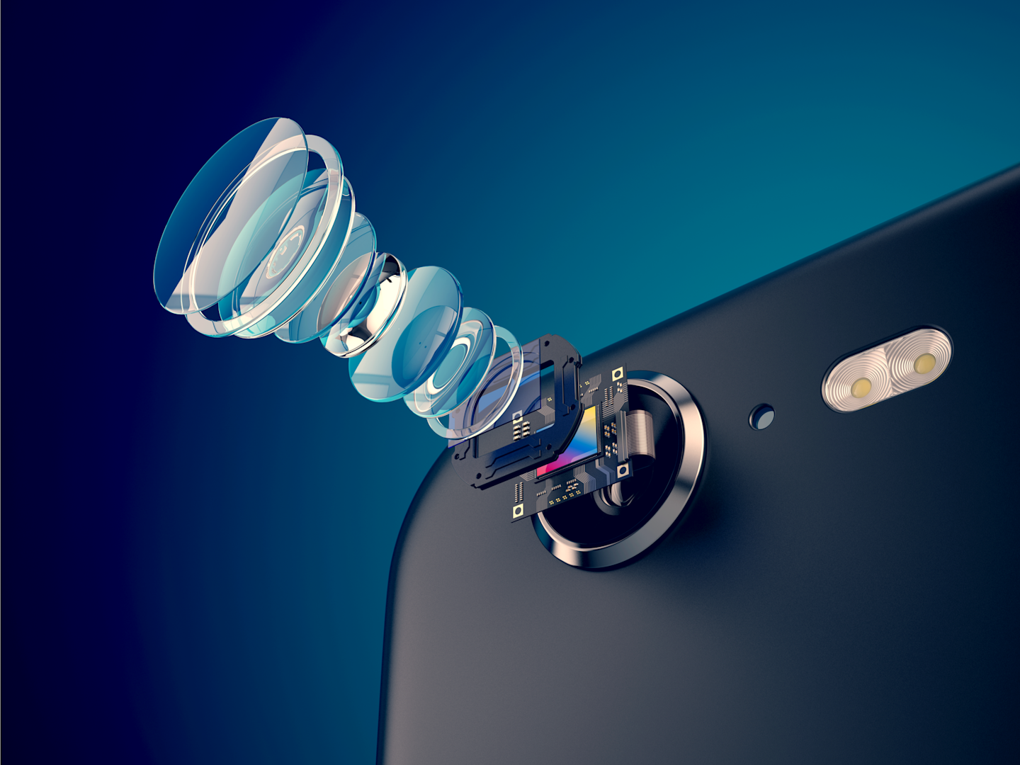
Why meta optics?
Meta optics is a technology which enables novel approaches to optical devices. To these include higher level of integration, combination of several optical functions to a single element, and new wafer level packaging. This novel technology also enables new optical sensing possibilities through additional degrees of freedom in optical design.

Key benefits of our approach
The technology, processes and materials we have developed permit
- Improved pattern fidelity
- Improved yield
- Long term optical performance
- Decoupling of pattering and optical performance

Benefits of the pattern transfer and etching of the substrate
Decoupling of the lithography and optical functional layers results in more freedom to optimize each layer and step separately. In this way optical performance is not limited e.g. by high refractive index imprintable materials.
Freedom to choose optical layers with high quality, high refractive index (e.g. low scattering, no yellowing) without residues of imprintable solutions. Pattern with precision to gain high yield and a cost benefit. Utilize advanced pattern transfer layers (hard masks ) to obtain high aspect ratio structures.
Company
We are an innovative materials company with strong R&D capabilities and a portfolio of unique patents. We are one of the only European suppliers of EUV lithography materials. Pibond’s materials have been adopted in the latest semiconductor devices globally. We enable, simplify, and increase the quality and performance of semiconductor and photonics devices.
Delivery Process
PiBond offers turn-key service from optical design to delivery of final components. We start with a feasibility analysis and modeling of the optical wave fronts. This is followed by a mask design and component fabrication. Finally, characterisation and singulation are carried out.

Substrates
- Silicon (Si)
- Gallium Nitride (GaN)
- Fused Quartz (SiO2)
- High index glass
Functional layers
- Titanium Dioxide (TiO2)
- Silicon Nitride (Si3N4)
- High refractive index polymer
- Metal oxide coating
Nanoimprinting (NIL) and lithography with etch transfer layers
Using nanoimprinting and photolithography as patterning methods. Pattern is transferred to the substrate or functional layer using oxygen (O2) or fluorine (F) / chlorine (Cl) based plasma etching of the etch transfer layers. Final structure can be overcoated if needed.

Materials and material engineering
Substrate
Functional layer
Hardmasks
Patterning
Strippers
AR-coating and overcoating
